|
||
| Products Download Events Support Videos | ||

Technical Support
On-Line Manuals
RL-ARM User's Guide (MDK v4)
NAND Page Data Layout
NAND Page Data Layout describes the NAND driver structure, the data organization in a NAND Flash device page, and methods to change the data organization.
The NAND driver configuration structure is defined in the file File_Config.h as follows:
typedef struct {
  NAND_PG_LAY* PgLay;                   /* Page Layout Definitions           */
  U16 NumBlocks;                        /* Number of blocks per device       */
  U16 NumPages;                         /* Number of pages per block         */
  U16 PageSize;                         /* Page size                         */
  U16 SectorsPerBlock;                  /* Number of sectors per block       */
  U8  SectorsPerPage;                   /* Number of sectors per page        */
  U8  AddrCycles;                       /* Device address cycles             */
  U8  SwEccEn;                          /* Software ECC enabled              */
  U8  DrvInst;                          /* Driver Instance definition        */
} const NAND_DRV_CFG;
The values set in the screen device configuration are propagated to this structure.
- PgLay
Pointer to the page data layout definition structure. This structure is filled with default layout definitions at FlashFS initialization. - NumBlocks
Number of blocks per device, as defined in the NAND Flash Drive configuration. - NumPages
Number of pages per block, as defined in the NAND Flash Drive configuration. - PageSize
Device page size, as defined in the NAND Flash Drive configuration. - SectorsPerBlock
Number of sectors per device block is derived from the device page size and number of pages per block. - SectorsPerPage
Number of sectors per device page is derived from device page size. - AddrCycles
Number of address cycles required for NAND device addressing. - SwEccEn
This variable is greater than zero if error correction code (ECC) encoding/decoding is enabled in software:
0 = Software ECC disabled
1 = Hamming ECC algorithm enabled in software. - DrvInst
Provides information about NAND flash drive instance number. This variable can be used to determine NAND device chip select. If only one NAND drive is used, this value equals to zero.
Page Layout Structure
The page layout structure is defined in the file File_Config.h as follows:
typedef struct {
  U8  Pos_LSN;                          /* LSN position                      */
  U8  Pos_COR;                          /* Data in page corrupted marker     */
  U8  Pos_BBM;                          /* Bad Block marker position         */
  U8  Pos_ECC;                          /* First byte of ECC                 */
  U16 SectInc;                          /* Column increment till next sector */
  U16 SpareOfs;                         /* Spare area offset from beginning  */
                                        /* of the page                       */
  U16 SpareInc;                         /* Column increment till next spare  */
} NAND_PG_LAY;
This structure contains basic configuration info:
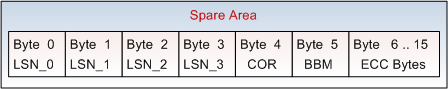
- Pos_LSN
Position in spare area, where logical sector number (LSN) is placed. Usually, this is the first byte of spare, therefore Pos_LSN has value zero. LSN is a 32-bit value. - Pos_COR
Position of data corrupted marker in spare area. Usually, this byte is the fifth byte of spare and Pos_COR has value four. - Pos_BBM
Position of bad block marker (BBM) in spare area and is usually placed as the sixth byte of spare, Pos_BBM has value 5. - Pos_ECC
Position of the first byte of Error Correction Code (ECC) bytes in the spare area. First ECC byte is default seventh byte of spare (Pos_ECC == 6). This value is used by flash translation layer only if ECC is encoded and decoded in software. - SectInc
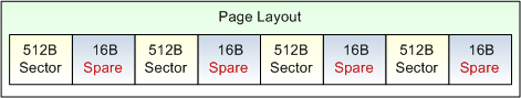
Provides information about user data sector locations within page. If page contains multiple sectors, first sector always starts at the beginning of the page (byte zero). Second sector starts at SectInc, third sector at SectInc + SectInc and so on. - SpareOfs
Provides information about the location of the first spare area byte within page. - SpareInc
Provides information about spare area locations within page. If page contains multiple sectors, first byte of the first spare area is determined by reading SpareOfs value. Location of the first byte of the second spare, can be determined by adding SpareInc value to the SpareOfs value.
The default page data layout (defined by SectInc, SpareOfs and SpareInc values) contains a Spare area after each sector.
Default 16-byte spare area data organization (defined by Pos_LSN, Pos_BBM and Pos_ECC values):
Changing the default page data layout
The NAND Flash device, or controller peripheral, can demand a different page data layout in order to calculate and store redundant error correction information. To alter the page data layout, overwrite the fields in the structure NAND_PG_LAY using the Init function.
The spare area for OneNAND device is located after the last sector in a page:
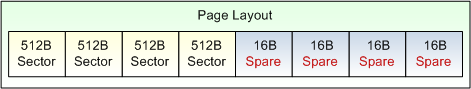
Page data layout example to support OneNAND devices:
static U32 Init (NAND_DRV_CFG *cfg) {

  /* Setup OneNAND Page Layout */
  cfg->PgLay->Pos_LSN  =    2;
  cfg->PgLay->Pos_COR  =    1;
  cfg->PgLay->Pos_BBM  =    0;
  cfg->PgLay->Pos_ECC  =    8;
  cfg->PgLay->SectInc  =  512;
  cfg->PgLay->SpareOfs = 2048;
  cfg->PgLay->SpareInc =   16;

  /* Init NAND Driver Peripheral */
  /*          ...                */
  return RTV_NOERR;
}
ProductsDevelopment Tools |
Hardware & Collateral |
Downloads |
Support |
Contact |