 |
File System Component
Version 6.16.6
MDK Middleware for Devices with Flash File System
|
|
File System Component
Version 6.16.6
MDK Middleware for Devices with Flash File System
|
NAND Flash memory is used in USB drives, secure digital (SD) cards, memory sticks, CompactFlash cards and multimedia cards (MMC). It is a non-volatile memory with 60 percent smaller memory cells comparing to NOR memory cells thus offers high data density at a lower cost. It is organized into a series of blocks, which are the smallest erasable entities in a NAND Flash device. The smallest entity that can be programmed is a byte. Due to a limited number of times NAND Flash blocks can be reliably programmed and erased (nominally, each NAND block will survive 100000 program/erase cycles) it is critical to implement a NAND Flash Translation Layer (NFTL) to maximize the lifespan of the device. This layer comprises of wear leveling algorithms, bad block management and error control algorithms and thus maximizes the lifespan of a device by redirecting new writes to different physical blocks. It only applies to NAND Flash devices directly attached to the microcontroller.
A NAND Flash array is organized in blocks with multiple pages per block. Each page consist of user data area and spare data area. The spare data area is physically the same as user data area and is typically used for error correction information (ECC), wear leveling and other software system functions. The user data area is available to the user for data storage. The size of the user data area depends on the page size and is typically of one or multiple sector size.
Due to its architecture, data can be written to an address on a NAND flash memory only a finite number of times. NAND flash memory wears out if data is written too often to the same address, so wear leveling is used to help prolong the life of the NAND flash device. It ensures that data erasures and writes are distributed evenly across the NAND Flash storage medium, so that NAND memory blocks don't fail prematurely due to a high number of erase cycles.
Dynamic wear leveling addresses the issue of repeated writes to the same logical blocks by redirecting new writes to different physical blocks. Dynamic wear leveling works on data blocks that are being written to dynamically.
Static wear leveling addresses the issue of static data that is kept unchanged for a long time in content and location. Some static data can stay in the same data block until the NAND flash memory is broken. To evenly distribute write and erase cycles across NAND memory blocks, an algorithm is implemented to move the static data from one location to the other in the Flash.
The File System Component implements wear leveling for all kinds of NAND Flash devices (SLC, MLC, TLC).
It is normal for a NAND flash memory to contain bad or invalid blocks of memory. Invalid blocks are blocks that contain one or more invalid bits so that the reliability can no longer be guaranteed. Blocks can become invalid during erasing and programming at run-time or during the manufacturing process. Bad blocks generated during manufacturing process are marked bad by the manufacturer. Bad blocks detected at run-time are marked as bad by monitoring the status register in the NAND flash chip during an erase and program operation. A block that is marked as bad is skipped and no longer used.
The File System Component implements bad block management for all kinds of NAND Flash devices (SLC, MLC, TLC):
Error detection and correction codes are used in flash memory to protect data from corruption. All types of error correction codes add redundant information to the data being stored to the flash memory. The redundant information is calculated before the data is written, added to the spare area of the page and then stored in flash memory. When the data is read, the redundant information is recalculated and compared to those stored in the flash.
Error correction codes (ECC) used in the NAND flash memory are block codes. This means that the redundant data bits are calculated for a fixed size block of used data. NTFL is implementing a Hamming ECC algorithm which is able to correct 1-bit and detect 2-bit errors for a fixed size of one sector or 512 bytes for SLC NAND Flashes. The redundant information is calculated in a way that a balance of correction power and efficiency is achieved.
On-Chip ECC is supported on EZ NAND compliant devices. Various ECC layouts are supported by using flexible ECC codeword configuration.
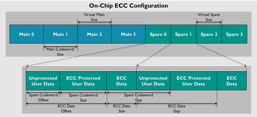
ECC algorithms typically operate on smaller sections of the NAND physical page size. This section can be described as ECC virtual page, with its main and spare part. Typically main part consists of 512 bytes while spare part can be of different sizes (16, 28, 32, etc. bytes).
Amount of protected data is defined by codeword size, which is typically 512 bytes in main area and of various sizes in spare. Spare codeword may also not be aligned to start of spare area, but is located in spare with some offset. Spare codewords may also follow each other in arbitrary order, therefore codeword gap defines the gap between each codeword. It is similar with generated ECC data - its size, offset from start of spare and gap between each other may be arbitrary.

