|
||
| Products Download Events Support Videos | ||

Technical Support
On-Line Manuals
MCBTSX1001 User's Guide
Jumper Descriptions
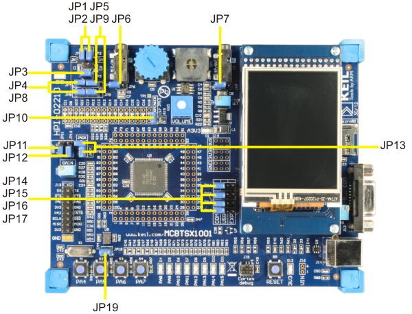
The jumpers used to configure the MCBTSX1001 board are:
- JP1 POT/JK/DIFF: Selects the analog input and amplifier configuration for negative FDA input for the ADC. The POT position selects the potentiometer (R2) for analog input. The JK position selects the MIC jack (J1) for input bypassing the LNA0 and LNA1. The DIFF position uses the MIC input (J1) also, but amplifies the MIC input via low-noise amplifiers LNA0 and LNA1.
- JP2 POT/JK/DIFF: Selects the analog input and amplifier configuration for positive FDA input for the ADC. The POT position selects the potentiometer (R2) for analog input. The JK position selects the MIC jack (J1) for input bypassing the LNA0 and LNA1. The DIFF position uses the MIC input (J1) also, but amplifies the MIC input via low-noise amplifiers LNA0 and LNA1.
- JP3: Grounds the negative input to FDOA1 when JP2 input bypasses LNA0 and LNA1.
- JP4 AOUT: Connects the positive output of FDOA0 to SEOA0 input. Pin 2 of JP4 may be jumpered to pin 1 of JP5 for DAC to ADC loopback testing.
- JP5 AIN: Connects the positive output of FDOA1 to the positive ADC input. Pin 1 of JP5 may be jumpered to pin 2 of JP4 for DAC to ADC loopback testing.
- JP6: Provides a 5 VDC microphone bias at MIC jack (J1).
- JP7 S/J: The S position selects the on-board speaker (SP1) for audio output. The J position selects the SP/OUT headphone jack for audio output.
- JP8 AOUT: Connects the negative output of FDOA0 to SEOA0 input. Pin 2 of JP8 may be jumpered to pin 1 of JP9 for DAC to ADC loopback testing.
- JP9 AIN: Connects the negative output of FDOA1 to the negative ADC input. Pin 1 of JP9 may be jumpered to pin 2 of JP8 for DAC to ADC loopback testing.
- JP10 SPEAKER: Connects the single-ended DAC data to LM386 audio amplifier.
- JP11 VREF 1/0: 0 supplies a 1.2 bandgap buffered voltage reference for FDOA1 and the MIC inputs. 1 supplies a VDD/2 buffered voltage reference for FDOA1 and the MIC inputs.
- JP12 VREF 1/0: 0 supplies a 1.2 bandgap buffered voltage reference for the single-ended amplifier SEOA0. 1 supplies a VDD/2 buffered voltage reference for the single-ended amplifier SEOA0.
- JP13 JACK: 2 jumpers connect the MIC jack (J1) to the low-noise amplifiers LNA0 and LNA1. You may remove these jumpers to attach an external cable to LNA0 and LNA1 input.
- JP14 RTS COM/USB/EXP: Connects the UART RTS signal to RTS on either the RS232 driver/receiver ST232E (COM), or the USB to serial FT232RQ (USB). The EXT position is for future interface expansion and has on-board connection.
- JP15 CTS COM/USB/EXP: Connects the UART CTS signal to CTS on either the RS232 driver/receiver ST232E (COM), or the USB to serial FT232RQ (USB). The EXT position is for future interface expansion and has on-board connection.
- JP16 RX COM/USB/EXP: Connects the UART RX signal to RX on either the RS232 driver/receiver ST232E (COM), or the USB to serial FT232RQ (USB). The EXT position is for future interface expansion and has on-board connection.
- JP17 TX COM/USB/EXP: Connects the UART TX signal to TX on either the RS232 driver/receiver ST232E (COM), or the USB to serial FT232RQ (USB). The EXT position is for future interface expansion and has on-board connection.
- JP19 OSC EN: Enables the 44mHz oscillator at U9.
ProductsDevelopment Tools |
Hardware & Collateral |
Downloads |
Support |
Contact |