|
||
| Products Download Events Support Videos | ||
Product Information
Device Database®
Downloads
Compliance Testing
Distributors
Peripheral Simulation
For Infineon XC2267M-56F — A/D Converter (16 channels)
Simulation support for this peripheral or feature is comprised of:
- Dialog boxes which display and allow you to change peripheral configuration.
- VTREGs (Virtual Target Registers) which support I/O with the peripheral.
These simulation capabilities are described below.
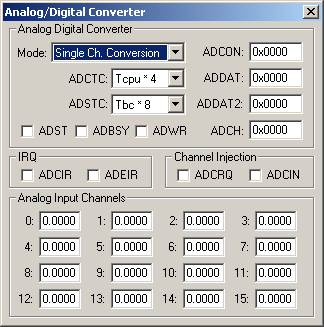
Analog/Digital Converter Dialog

The Analog/Digital Converter dialog displays and allows you to edit the configuration of the A/D converter. The controls in this dialog are separated into several logical groups.
The Analog Digital Converter group contains the following controls.
- Mode displays and allows you to change the A/D Converter mode of operation.
- ADCTC displays and allows you to select the A/D Converter time control.
- ADSTC displays and allows you to select the A/D Converter sample time control.
- ADST is the A/C Converter start control flag.
- ADBSY is the busy flag. It indicates that a conversion is in progress.
- ADWR is the wait for read control flag.
- ADCON is the A/D Converter Control Register (SFR).
- ADDAT is the A/D Converter Result Register (SFR).
- ADDAT2 is the A/D Converter Channel Injection Register (SFR).
- ADCH specifies the first A/D channel to convert.
The IRQ group contains the following controls.
- ADCIR is the A/D Converter interrupt request flag.
- ADEIR is the A/D Converter error interrupt request flag.
The Channel Injection group contains the following controls.
- ADCRQ is the A/D Converter channel injection request flag.
- ADCIN is the A/D Converter channel injection enable flag.
The Analog Input Channels group contains an input box for each analog channel is displayed at the bottom of the dialog. These boxes display the current voltage for the channel. You may edit the value to specify a new input voltage for that channel. When the A/D Converter subsequently performs a conversion using that channel, the input voltage specified is converted into a digital value.
AINx VTREG
Data Type: float
The AINx VTREGs set the analog input voltages for simulated A/D converters. The AINx VTREGs represent the inputs to the analog input pins of the MCU for analog input 0, 1, 2, and so on. AIN0 sets the input voltage for analog input #0, AIN1 sets the input voltage for analog input #1, etc. If you have properly configured the analog inputs, the following commands (typed in the debugger's Command Window) input the voltages specified.
AIN0 = 0.000  /* Analog Input 0 = 0.000 volts */
AIN1 = 2.500  /* Analog Input 1 = 2.500 volts */
AIN2 = 4.999  /* Analog Input 2 = 4.999 volts */
You may create a debugger signal function to periodically change the value of the A/D input. The following signal function increases the A/D Channel 1 input voltage by 0.1 volts each second.
signal void AIN1_sig (void) {
float f;

for (f = 0.0; f < 5.0; f += 0.1)
  {
  swatch (1.0);                  // Delay 1 second
  AIN1 = f;                      // Set AIN1 Voltage
  }
}
ProductsDevelopment Tools |
Hardware & Collateral |
Downloads |
Support |
Contact |
