|
||
| Products Download Events Support Videos | ||
Product Information
Device Database®
Downloads
Compliance Testing
Distributors
Peripheral Simulation
For Hynix Semiconductor GMS97C2051 — Analog Comparator
Simulation support for this peripheral or feature is comprised of:
- Accurate simulation of special on-chip features.
- Dialog boxes which display and allow you to change peripheral configuration.
- VTREGs (Virtual Target Registers) which support I/O with the peripheral.
These simulation capabilities are described below.
Analog Comparator
The AT89C1051, AT89C2051 and AT89C4051 MCUs support an on-chip Analog Comparator. This comparator uses AIN0 (P1.0) and AIN1 (P1.1) input pins for analog input and uses bit 6 of Port 3 (P3.6) for the comparator output result. Because of this, P3.6 is not available for general purpose I/O. The MCU sets the comparator output (P3.6) to 1 when the analog input AIN0 (P1.0) is greater than or equal to the analog input AIN1 (P1.1).
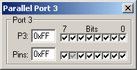
Port 3 Dialog

This dialog displays the SFR and pins of Port 3.
- P3: This is the P3 SFR. The HEX value and value of each bit is displayed and may be changed from this dialog.
- Pins: These are the states of the pins on the simulated MCU. When used as outputs, these have the same value as the P3 SFR. When used as inputs (P3.x is 1) you may set the level of the input pin to high (1) or low (0). P3.6 may not be used for general purpose I/O. It is internally connected to the Analog Comparator output.
The PORT3 VTREG may be used (from the Command Window or from a user or signal function) to affect the input values of the simulated pins of Port 3.
AINx VTREG
Data Type: float
The AINx VTREGs set the analog input voltages for simulated A/D converters. The AINx VTREGs represent the inputs to the analog input pins of the MCU for analog input 0, 1, 2, and so on. AIN0 sets the input voltage for analog input #0, AIN1 sets the input voltage for analog input #1, etc. If you have properly configured the analog inputs, the following commands (typed in the debugger's Command Window) input the voltages specified.
AIN0 = 0.000  /* Analog Input 0 = 0.000 volts */
AIN1 = 2.500  /* Analog Input 1 = 2.500 volts */
AIN2 = 4.999  /* Analog Input 2 = 4.999 volts */
You may create a debugger signal function to periodically change the value of the A/D input. The following signal function increases the A/D Channel 1 input voltage by 0.1 volts each second.
signal void AIN1_sig (void) {
float f;

for (f = 0.0; f < 5.0; f += 0.1)
  {
  swatch (1.0);                  // Delay 1 second
  AIN1 = f;                      // Set AIN1 Voltage
  }
}
ProductsDevelopment Tools |
Hardware & Collateral |
Downloads |
Support |
Contact |
