|
||
| Products Download Events Support Videos | ||
Product Information
Device Database®
Downloads
Compliance Testing
Distributors
Peripheral Simulation
For NXP (founded by Philips) LPC1766 — Clocking & Power Control
Simulation support for this peripheral or feature is comprised of:
- Dialog boxes which display and allow you to change peripheral configuration.
These simulation capabilities are described below.
Clkout Clock Selection Dialog
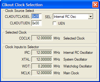
The Clkout Clock Selection dialog selects the source of the input clocking from the 3 independent oscillators.
Clock Source Select
- CLKOUTCLKSEL (Clock Output Clock Select Register) configures the clkout_clk signal to be output on the CLKOUT pin.
- CLKOUTUEN (CLKOUT Source Update Enable Register) holds the update clock source enable bit setting.
- UEN checkbox sets or resets the update clock source enable bit.
Selected Clock
- COCLK displays the selected clock output value.
Clock Inputs to Selector
- Oscillators IRC, XTAL, WDT and MCLK display the frequency of each clock source.
Clock Generation Schematic Dialog
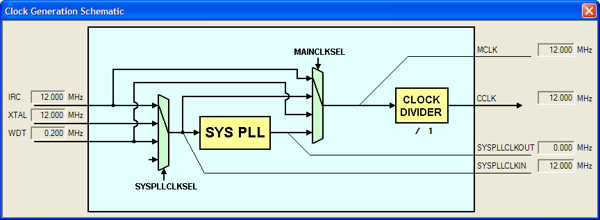
The Clock Generation Schematic displays input clock values and the resulting generated clock values to be used by the application.
Clock generation Schematic
- IRC is the on-chip 12 MHz oscillator.
- XTAL is the value of the external crystal.
- WDT is the watchdog timer source clock value.
- MCLK is the generated main clock.
- CCLK is the generated core clock.
- SYSPLLCLKOUT is the resulting system PLL clock.
- SYSPLLCLKIN is the input clock for the system PLL.
Phase Locked Loop 0 (PLL0) Dialog
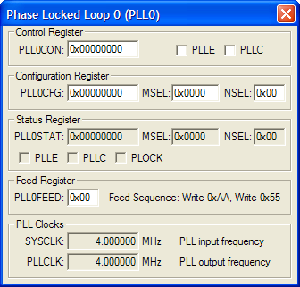
The Phase Locked Loop 0 Dialog controls Phase Locked Loop (PLL) function of the ARM controller. Using this dialog, you can configure the MCU clock frequency by changing the multiplier and divider values that control the MCU clock.
Control Register
- PLL0CON (PLL Control Register) contains the PLL Enable bit (bit 0), and the PLL Connect bit (bit 1).
- PLLE (PLL Enable) is set to activate the PLL and allow it to lock to the requested frequency.
- PLLC (PLL Connect) is set to connect the PLL as the clock source. A successful connect requires the PLLE bit set.
Configuration Register
- PLL0CFG (PLL Configuration Register) contains the PLL Multiplier (MSEL) and PLL Divider (PSEL) values.
- MSEL (PLL Multiplier Value) is the multiplier value used in calculating the PLL clock frequency.
- PSEL (PLL Divider Value) is the divider value used in calculating the PLL clock frequency.
Status Register
- PLL0STAT (PLL Status Register) contains the following PLL status bits:
- MSEL (PLL Multiplier Read-Back Value) is the multiplier value currently used by the PLL.
- PSEL (PLL Divider Read-Back Value) is the divider value currently used by the PLL.
- PLLE (PLL Enable Read-Back Value) is set when the PLL is active. If reset, the PLL is turned off.
- PLLC (PLL Connect Read-Back Value) is set when the MCU uses the PLL as the clock source. If reset, the MCU uses the oscillator clock as the source.
- PLOCK (PLL Lock Status) is set when the PLL is locked on the requested frequency.
Feed Register
- PLL0FEED (PLL Feed Register) contains the 8-bit value last written to this register. To set the clock configuration, this register must be stored with consecutive values of 0xAA and 0x55, while the PLLE and PLLC bits are enabled.
Crystal Oscillator & Processor Clock
- XTAL (Crystal Oscillator Frequency) the frequency (in MHz) of the crystal oscillator.
- CLOCK (Processor Clock) is the computed processor clock frequency (CCLK) in MHz.
Phase Locked Loop 1 (PLL1) Dialog
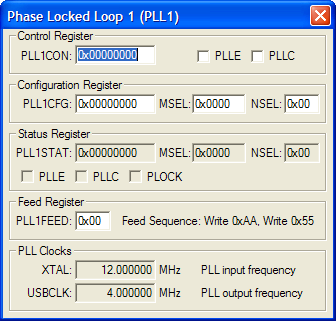
The Phase Locked Loop 1 Dialog controls Phase Locked Loop (PLL) function of the ARM controller. Using this dialog, you can configure the MCU clock frequency by changing the multiplier and divider values that control the MCU clock.
Control Register
- PLL1CON (PLL Control Register) contains the PLL Enable bit (bit 0), and the PLL Connect bit (bit 1).
- PLLE (PLL Enable) is set to activate the PLL and allow it to lock to the requested frequency.
- PLLC (PLL Connect) is set to connect the PLL as the clock source. A successful connect requires the PLLE bit set.
Configuration Register
- PLL1CFG (PLL Configuration Register) contains the PLL Multiplier (MSEL) and PLL Divider (PSEL) values.
- MSEL (PLL Multiplier Value) is the multiplier value used in calculating the PLL clock frequency.
- PSEL (PLL Divider Value) is the divider value used in calculating the PLL clock frequency.
Status Register
- PLL1STAT (PLL Status Register) contains the following PLL status bits:
- MSEL (PLL Multiplier Read-Back Value) is the multiplier value currently used by the PLL.
- PSEL (PLL Divider Read-Back Value) is the divider value currently used by the PLL.
- PLLE (PLL Enable Read-Back Value) is set when the PLL is active. If reset, the PLL is turned off.
- PLLC (PLL Connect Read-Back Value) is set when the MCU uses the PLL as the clock source. If reset, the MCU uses the oscillator clock as the source.
- PLOCK (PLL Lock Status) is set when the PLL is locked on the requested frequency.
Feed Register
- PLL1FEED (PLL Feed Register) contains the 8-bit value last written to this register. To set the clock configuration, this register must be stored with consecutive values of 0xAA and 0x55, while the PLLE and PLLC bits are enabled.
Crystal Oscillator & Processor Clock
- XTAL (Crystal Oscillator Frequency) the frequency (in MHz) of the crystal oscillator.
- CLOCK (Processor Clock) is the computed processor clock frequency (CCLK) in MHz.
Power Control Dialog
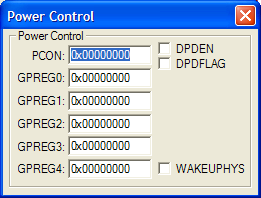
The Power Control Dialog controls the power saving mode of the ARM controller. With this dialog, you can selectively enable or disable unused peripherals to save power.
Power Control
- PCON (Power Control Register) contains the DPDEN and DPDFLAG bits.
- DPDEN (Deep Power-down Mode Enable) enables deep power-down mode when an ARM/Cortex-M0 WFI/WFE instruction is executed.
- DPDFLAG (Deep Power-down Mode Flag) if set, indicates the device is in deep power-down mode.
- GPREGn (General Purpose Register n) colds data retained during deep power-down mode. GPREG4 hold the WAKEUPHYS setting.
- WAKEUPHYS (WAKEUP Pin Hysteresis Enable) if set, enables hysteresis for the WAKEUP pin.
ProductsDevelopment Tools |
Hardware & Collateral |
Downloads |
Support |
Contact |
