|
||
| Products Download Events Support Videos | ||
Product Information
Device Database®
Downloads
Compliance Testing
Distributors
Peripheral Simulation
For STMicroelectronics STR911FAW42 — Analog/Digital Converter (ADC)
Simulation support for this peripheral or feature is comprised of:
- Dialog boxes which display and allow you to change peripheral configuration.
- VTREGs (Virtual Target Registers) which support I/O with the peripheral.
These simulation capabilities are described below.
Analog/Digital Converter Dialog

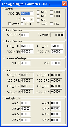
The Analog / Digital Converter dialog displays and configures the A/D converter. The controls in this dialog are separated into several logical groups.
Control
- ADC_CR (ADC Control Register) contains the following control and status settings:
- SC (Channel Address) selects the channel to be sampled when external addressing (AXT) is enabled.
- AWDI (Analog Watchdog Interrupt Enable) is set to enable the analog watchdog feature.
- ECVI (End of Conversion Interrupt Enable) is set to enable the end of conversion interrupt.
- STR (Start Conversion) is set to start ADC conversion.
- STB (Standby Mode Enable) is set to put the analog block in low power mode.
- SCE (Scan Mode Enable) is set to convert all ADC channels.
- AWD (Analog Watchdog Flag) is set to indicate an analog watchdog event occurred.
- POR (Power On/Reset Mode) when set, ADC digital block is running and analog block is in standby mode. When reset, analog block is off.
- CONT (Continuous Mode Enable) is set to indicate continuous mode. If reset, the ADC runs in one-shot mode.
- ECV (End oc Conversion Flag) is set to indicate the ADC conversion is complete.
Clock Prescaler
- ADC_PRS ()
- Fmod(Hz) (Modulator Oversampling Frequency) is the sampling frequency input to the ADC.
- ADC_CCR (ADC Prescaler Control Register)
- ADC_HTR ()
- ADC_CRR ()
- ADC_LTR ()
Reference Voltage
- VREF is the feedback reference voltage used for the ADC.
- VDD is the chip power voltage.
Data
- ADC_DRn (ADC Data Register) contains the raw converted result of the ADC conversion for channel n.
Analog Inputs
- ADCn (Analog Input) contains the simulated analog input voltage (VTREG ADCn) for channel n.
ADCx Input Voltage VTREG
Data Type: float
The ADCx VTREGs set the analog input voltages for simulated A/D converters. The ADCx VTREGs represent the inputs to the analog input pins of the MCU for analog input 0, 1, 2, and so on. ADC0 sets the input voltage for analog input #0, ADC1 sets the input voltage for analog input #1, etc. If you have properly configured the analog inputs, the following commands (typed in the debugger's Command Window) input the voltages specified.
ADC0 = 0.000  /* Analog Input 0 = 0.000 volts */
ADC1 = 2.500  /* Analog Input 1 = 2.500 volts */
ADC2 = 4.999  /* Analog Input 2 = 4.999 volts */
You may create a debugger signal function to periodically change the value of the A/D input. The following signal function increases the A/D Channel 1 input voltage by 0.1 volts each second.
signal void ADC1_sig (void) {
float f;

for (f = 0.0; f < 5.0; f += 0.1)
  {
  swatch (1.0);                  // Delay 1 second
  ADC1 = f;                      // Set ADC1 Voltage
  }
}
ProductsDevelopment Tools |
Hardware & Collateral |
Downloads |
Support |
Contact |
