|
||
| Products Download Events Support Videos | ||
Product Information
Device Database®
Downloads
Compliance Testing
Distributors
Peripheral Simulation
For Infineon XC878M-16FF — Port 0
Simulation support for this peripheral or feature is comprised of:
- Dialog boxes which display and allow you to change peripheral configuration.
- VTREGs (Virtual Target Registers) which support I/O with the peripheral.
These simulation capabilities are described below.
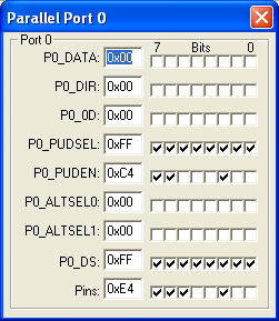
Parallel Port 0 Dialog

This dialog displays the SFR and pins of Port 0. This port has several alternate functions but it may be used as a 8-bit general purpose I/O port.
- P0_DATA represents the P0 SFR. The HEX value and value of each bit is displayed and may be changed from this dialog.
- P0_DIR is the port direction SFR for P0_DATA. When P0_DIR.x=0, P0_DATA.x is an input. When P0_DIR.x=1, P0_DATA.x is an output.
- P0_OD is the open drain control SFR for P0_DATA. When P0_OD.x=0, the P0_DATA.x output driver works in push/pull mode. When P0_OD.x=1, the P0_DATA.x output driver works in open drain mode.
- P0_PUDSEL selects a pull-up or pull-down device for each pin in P0_DATA. When P0_PUDSEL.x=0, P0_DATA.x is pulled down. When P0_PUDSEL.x=1, P0_DATA.x is pulled up(default).
- P0_PUDEN enables a pull-up or pull-down devices for each pin in P0_DATA. When P0_PUDEN.x=0, P0_PUDSEL.x is disabled. When P0_PUDEN.x=1, P0_PUDSEL.x is enabled.
- P0_ALTSEL0 selects the general purpose I/O, Alternate Output 1.
- P0_ALTSEL1 selects the general purpose I/O, Alternate Output 2.
- Pins represents the states of the pins on the simulated MCU. When used as outputs, these have the same value as the P0_DATA SFR. When used as inputs (P0_DIR.x is 0) you may set the level of the input pin to high (1) or low (0).
PORTx VTREG
Data Type: unsigned char
The PORTx VTREGs represent the I/O pins of the simulated MCU for Port 0, Port 1, and so on. PORT0 represents Port 0, PORT1 represents Port 1, etc. You may read PORTx to determine the state of the output pins of that port. For example, in the command window, you may type,
PORT0
to obtain value corresponding to the set pins of Port 0. You may also change the input values of port pins by changing the value of the VTREG. For example,
PORT1=0xF0
sets the upper four port pins of Port 1 to a value of 1 and the lower 4 port pins to a value of 0. You may use the bitwise operators AND(&), OR(|) and XOR(^) to change individual bits of the PORTx VTREGs. For example:
PORT1 |=  0x01;  /* Set P1.0 Pin */
PORT3 &= ~0x02;  /* Clr P3.1 Pin */
PORT1 ^=  0x80;  /* Toggle P1.7 Pin */
ProductsDevelopment Tools |
Hardware & Collateral |
Downloads |
Support |
Contact |
