|
||
| Products Download Events Support Videos | ||
Product Information
Device Database®
Downloads
Compliance Testing
Distributors
Peripheral Simulation
For STMicroelectronics STR750FV0 — Analog/Digital Converter (ADC)
Simulation support for this peripheral or feature is comprised of:
- Dialog boxes which display and allow you to change peripheral configuration.
- VTREGs (Virtual Target Registers) which support I/O with the peripheral.
These simulation capabilities are described below.
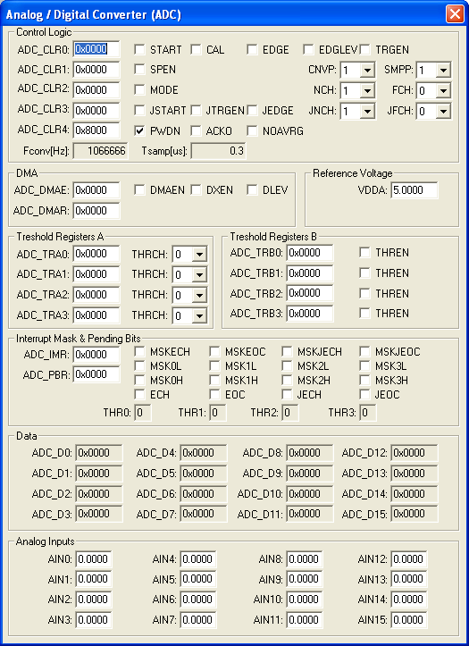
Analog / Digital Converter Dialog

The Analog / Digital Converter dialog displays and configures the A/D converter. The controls in this dialog are separated into several logical groups.
Control and Status
- ADC_CSR (ADC Control & Status Register) contains the following control and status settings:
- A (Channel Address) selects the channel to be sampled when external addressing (AXT) is enabled.
- OR (Overrun) is set when one of the data channels is overwritten before being read.
- AXT (Addressing External Enable) is set to allow single-channel conversion. If reset, channels are addressed in a round-robin fashion.
- IEn (Interrupt Enable - Channel n) is set to enable interrupts for the corresponding channel n.
- DAn (Data Available - Channel n) is set when new sample data is ready to be read for channel n.
Prescaler
- ADC_CPR (ADC Prescaler Register) contains the following prescaler settings:
- PRESC (Prescaler Value) is the 12-bit PCLK2 clock divisor used to produce the oversampling clock.
- Fmod(Hz) (Modulator Oversampling Frequency) is the sampling frequency input to the ADC.
- Rate(Hz) (Modulator Oversampling Rate) is oversampling rate based on the prescaling factor (PRESC).
Data
- ADC_DATAn (ADC Data Register) contains the raw converted result of the ADC conversion for channel n.
- DATAn (Converted Data) contains the converted data value for channel n.
Analog Inputs
- AINn (Analog Input) contains the simulated analog input voltage (VTREG AINn) for channel n.
Reference & Center
- VREF is the feedback reference voltage used for the ADC.
- VCM is the midpoint between the voltage range of the ADC converter and the feedback reference voltage (VREF).
AINx Input Voltage VTREG
Data Type: float
The AINx VTREGs set the analog input voltages for simulated A/D converters. The AINx VTREGs represent the inputs to the analog input pins of the MCU for analog input 0, 1, 2, and so on. AIN0 sets the input voltage for analog input #0, AIN1 sets the input voltage for analog input #1, etc. If you have properly configured the analog inputs, the following commands (typed in the debugger's Command Window) input the voltages specified.
AIN0 = 0.000  /* Analog Input 0 = 0.000 volts */
AIN1 = 2.500  /* Analog Input 1 = 2.500 volts */
AIN2 = 4.999  /* Analog Input 2 = 4.999 volts */
You may create a debugger signal function to periodically change the value of the A/D input. The following signal function increases the A/D Channel 1 input voltage by 0.1 volts each second.
signal void AIN1_sig (void) {
float f;

for (f = 0.0; f < 5.0; f += 0.1)
  {
  swatch (1.0);                  // Delay 1 second
  AIN1 = f;                      // Set AIN1 Voltage
  }
}
VREF Voltage VTREG
Data Type: unsigned short
ProductsDevelopment Tools |
Hardware & Collateral |
Downloads |
Support |
Contact |
