|
||
| Products Download Events Support Videos | ||
Product Information
Device Database®
Downloads
Compliance Testing
Distributors
Peripheral Simulation
For NXP (founded by Philips) LPC2364 — A/D Converter (8-Channels)
Simulation support for this peripheral or feature is comprised of:
- Dialog boxes which display and allow you to change peripheral configuration.
- VTREGs (Virtual Target Registers) which support I/O with the peripheral.
These simulation capabilities are described below.
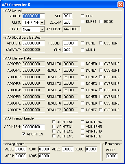
A/D Converter Dialog

The A/D Converter dialog displays the status registers for all of the A/D converters supported by this device. The Analog Input Channels, listed at the bottom of the dialog, allow you to specify the voltage for each analog input.
A/D Control
- ADCR (A/D Control Register) contains the following control bits for the A/D controller:
- CLKS (Conversion Clocks)selects the number of clocks used for each conversion in Burst mode and the bit accuracy.
- START controls when and if the an A/D conversion is started.
- SEL selects which pins of the analog input (AINn) are to be sampled and converted.
- CLKDIV (Clock Divisor) is the value (minus 1) divided into the VPB clock to produce the A/D Rate.
- A/D Rate displays the A/D clock rate.
- PDN (Power Down) is set if the A/D is operational. When reset, the A/D is in power down mode.
- BURST is set to use the number of clocks specified in BURST. If reset, conversions are software controlled and requires 11 clocks.
- EDGE is set to start the conversion on a rising edge. If reset, conversion starts on a falling edge.
A/D Data
- ADDR (A/D Data Register) contains the following bits for controlling A/D data conversion:
- CHN (Channel) is the channel containing the converted bits.
- V3A (Analog 3.3 Volts) input power voltage typically the same as V3 but may be isolated to reduce noise.
- V/V3A contains the current AINn result divided by the analog input power pin.
- DONE is set when the A/D conversion completes.
- OVERRUN is set if one or more conversions were overwritten before the current conversion completed.
Analog Inputs
- AINn (Analog Input Channels n) are used for setting voltage input to the ADC. These inputs are alternate functions for Port pins. The text box displays the analog voltage value for each input channel.
AINx VTREG
Data Type: float
The AINx VTREGs set the analog input voltages for simulated A/D converters. The AINx VTREGs represent the inputs to the analog input pins of the MCU for analog input 0, 1, 2, and so on. AIN0 sets the input voltage for analog input #0, ADC1 sets the input voltage for analog input #1, etc. If you have properly configured the analog inputs, the following commands (typed in the debugger's Command Window) input the voltages specified.
AIN0 = 0.000  /* Analog Input 0 = 0.000 volts */
AIN1 = 2.500  /* Analog Input 1 = 2.500 volts */
AIN2 = 4.999  /* Analog Input 2 = 4.999 volts */
You may create a debugger signal function to periodically change the value of the A/D input. The following signal function increases the A/D Channel 1 input voltage by 0.1 volts each second.
signal void AIN1_sig (void) {
float f;

for (f = 0.0; f < 5.0; f += 0.1)
  {
  swatch (1.0);                  // Delay 1 second
  AIN1 = f;                      // Set AIN1 Voltage
  }
}
ProductsDevelopment Tools |
Hardware & Collateral |
Downloads |
Support |
Contact |
