|
||
| Products Download Events Support Videos | ||
Product Information
Device Database®
Downloads
Compliance Testing
Distributors
Peripheral Simulation
For Infineon XC164S-32F — A/D Converter (14 channels)
Simulation support for this peripheral or feature is comprised of:
- Dialog boxes which display and allow you to change peripheral configuration.
- VTREGs (Virtual Target Registers) which support I/O with the peripheral.
These simulation capabilities are described below.
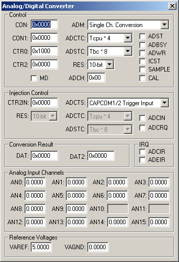
Analog/Digital Converter Dialog

The Analog/Digital Converter dialog displays and allows you to edit the configuration of the A/D converter. The controls in this dialog are separated into several logical groups.
Control
- CON (ADC Control Register) contains the ADCTC, ADSTC, ADCRQ, ADCIN, ADWR, ADBSY, ADST, ADM and ADCH control bit settings used when in Compatibility Mode (MD bit is reset).
- CON1 (ADC Control Register 1) contains the ICST SAMPLE CAL, RES ADCTC and ADSTC control bit settings used when in Compatibility Mode (MD bit is reset).
- CTR0 (ADC Control Register 0) contains the MD, SAMPLE, ADCTS, ADCRQ, ADCIN, ADWR, ADBSY, ADST, ADM, CALOFF and ADCH control bit settings use when Enhanced Mode is enabled (MD bit is set).
- CTR2 (ADC Control Register 2) contains the RES ADCTC and ADSTC control bit settings use when Enhanced Mode is enabled (MD bit is set).
- MD (Mode Control) is set for Enhanced Mode, and reset for Compatibility Mode.
- ADM (ADC Mode Selection) displays and allows you to change the A/D Converter mode of operation (Fixed or Auto, Single or Continuous Scan.
- ADCTC (ADC Conversion Time Control) displays and allows you to select the A/D Converter time control.
- ADSTC (ADC Sample Time Control) displays and allows you to select the A/D Converter sample time control.
- RES (Conversion Resolution Control) is set for 8-bit resolution, and reset for 10-bit resolution.
- ADCH (Analog Channel Input Selection) specifies the first A/D channel to convert.
- ADST (ADC Start Bit) is set to start the ADC conversion.
- ADBSY (ADC Busy Flag) is set by the ADC to indicate that a conversion is in progress.
- ADWR (ADC Wait for Read Control) is set for use during continuous conversion, to wait for the previous conversion result to be read before starting the next conversion cycle.
- ICST (Improved Conversion and Sample Timing) is set to use a 6-bit field, rather than a 2-bit field for conversion and sample time control.
- SAMPLE (Sample Phase Status Flag) is set when the ADC is in the sample phase.
- CAL (Reset Calibration Phase Status Flag) is set when the ADC is in calibration the phase.
Injection Control
- ADCIN (ADC Channel Injection Enable) is set when A/D Converter channel injection is enabled.
- ADCRQ (ADC Channel Injection Request Flag) is set when A/D Converter channel injection is requested.
Conversion Result
- DAT (ADC Result Register) contains the 4-bit channel number and converted digital value (8-bits or 10-bits) for that channel.
- DAT2 (ADC Channel Injection Result Register) contains the 4-bit injected channel number and converted digital value (8-bits or 10-bits) for that injected channel.
IRQ
- ADCIR (A/D Converter Interrupt Request Flag) is set when a conversion is complete.
- ADEIR (A/D Converter Error Interrupt Request Flag) is set when a new conversion is complete and the previous conversion result was not read.
The Analog Input Channels group contains an input box for each analog channel is displayed at the bottom of the dialog. These boxes display the current voltage for the channel. You may edit the value to specify a new input voltage for that channel. When the A/D Converter subsequently performs a conversion using that channel, the input voltage specified is converted into a digital value. Reference Voltages
- VAREF is the analog input reference voltage.
- VAGND is the analog input ground voltage.
AINx VTREG
Data Type: float
The AINx VTREGs set the analog input voltages for simulated A/D converters. The AINx VTREGs represent the inputs to the analog input pins of the MCU for analog input 0, 1, 2, and so on. AIN0 sets the input voltage for analog input #0, AIN1 sets the input voltage for analog input #1, etc. If you have properly configured the analog inputs, the following commands (typed in the debugger's Command Window) input the voltages specified.
AIN0 = 0.000  /* Analog Input 0 = 0.000 volts */
AIN1 = 2.500  /* Analog Input 1 = 2.500 volts */
AIN2 = 4.999  /* Analog Input 2 = 4.999 volts */
You may create a debugger signal function to periodically change the value of the A/D input. The following signal function increases the A/D Channel 1 input voltage by 0.1 volts each second.
signal void AIN1_sig (void) {
float f;

for (f = 0.0; f < 5.0; f += 0.1)
  {
  swatch (1.0);                  // Delay 1 second
  AIN1 = f;                      // Set AIN1 Voltage
  }
}
ProductsDevelopment Tools |
Hardware & Collateral |
Downloads |
Support |
Contact |
