|
||
| Products Download Events Support Videos | ||
Product Information
Device Database®
Downloads
Compliance Testing
Distributors
Peripheral Simulation
For STMicroelectronics STR731FV0 — Pulse Width Modulators (PWM0-PWM5)
Simulation support for this peripheral or feature is comprised of:
- Dialog boxes which display and allow you to change peripheral configuration.
- VTREGs (Virtual Target Registers) which support I/O with the peripheral.
These simulation capabilities are described below.
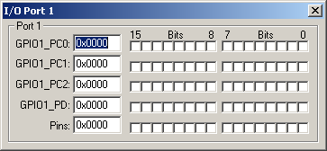
I/O Port 1 Dialog

The GPIO Port 1 Dialog controls the direction of the general purpose port pins. You may use the following controls to select and configure the GPIO port settings.
Port 1
- GPIO_PC0 - GPIO_PC2 (Port Bit Configuration Registers) specify how each I/O Port bit is configured (input, output, alternate function, etc.
- GPIO_PD checkboxes represent the data bits output.
- Pins allows you to manually set or clear individual pins for this port.
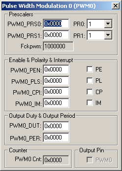
Pulse Width Modulation Dialog

The Pulse Width Modulator dialog configures Pulse Width Modulator (PWM) simulation.
Prescalers
- PWM0_PRS0 (PWM Prescaler 0) contains the divider factor (1, 2, 4, 8,..., 128) applied to the input clock.
- PR0 (Prescaler Register 0) selects the value (0-7) that corresponds to the primary divider factor (0=1, 1=2, 2=4, 3=8,..., 7=128).
- PWM0_PRS1 (PWM Prescaler 1) contains the divider factor (1-32)applied to the output of the the first prescaler.
- PR1 (Prescaler Register 1) selects the value (0-31) that corresponds to the secondary divider factor.
Enable & Polarity Interrupt
- PWM0_PEN (PWM Enable Register) contains the PWM Enable Register contents.
- PE (PWM Enable) is set to enable the PWM.
- PWM0_PLS (PWM Output Polarity Selection Register) controls the polarity (inverted or not inverted) of the PWM output.
- PL (PWM Polarity) is set to invert the PWM output.
- PWM0_CPI (PWM Compare Period Interrupt Register) contains the Compare Period Interrupt bit (CP) bit.
- CP (PWM Compare Period) is set to indicate that the compare register value has been reached.
- PWM0_IM (PWM Interrupt Mask Register) contains the Compare Period Interrupt Mask bit (IM) bit.
- IM (PWM Interrupt Mask) is set to enable the PWM interrupt.
Output Duty & Output Period
- PWM0_DUT (PWM Output Duty Register) contains the number of clocks that the output signal is at a high level, or low if polarity is inverted.
- PWM0_PER (PWM Output Period Register) contains the number of clocks that define the length of the entire PWM cycle.
Digital I/O Ports 0-2 (16-Bit) VTREG
Data Type: unsigned short
The PORTx VTREGs represent the I/O pins of the simulated MCU for Port 0, Port 1, and so on. PORT0 represents Port 0, PORT1 represents Port 1, etc. You may read PORTx to determine the state of the output pins of that port. For example, in the command window you may type,
PORT0
to obtain value corresponding to the set pins of Port A. You may also change the input values of port pins by changing the value of the VTREG. For example,
PORT0=0x000000F0
sets the upper four port pins of Port 0 to a value of 1 and all other port pins to a value of 0. You may use the bitwise operators AND(&), OR(|) and XOR(^) to change individual bits of the PORTx VTREGs. For example:
PORT0 |=  0x00000001;  /* Set P0.0 Pin */
PORT1 &= ~0x00000200;  /* Clr P1.9 Pin */
PORT0 ^=  0x00800000;  /* Toggle P0.23 Pin */
ProductsDevelopment Tools |
Hardware & Collateral |
Downloads |
Support |
Contact |
