|
||
| Products Download Events Support Videos | ||
Product Information
Device Database®
Downloads
Compliance Testing
Distributors
Peripheral Simulation
For Silicon Laboratories, Inc. C8051F067 — A/D Converter (2x16-bit)
Simulation support for this peripheral or feature is comprised of:
- Dialog boxes which display and allow you to change peripheral configuration.
- VTREGs (Virtual Target Registers) which support I/O with the peripheral.
These simulation capabilities are described below.
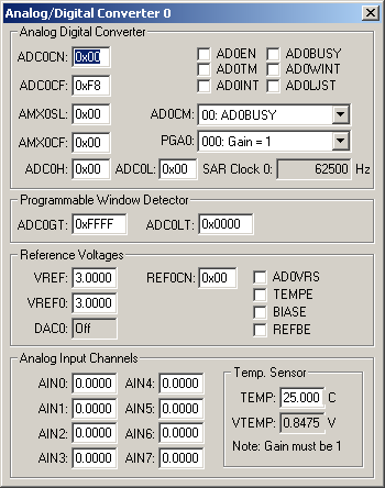
Analog/Digital Converter 0 Dialog

The Analog/Digital Converter (ADC) dialog displays and configures the A/D converter. The controls in this dialog are separated into several logical groups.
Analog Digital Converter
- ADC0CN contains the following ADC control register settings:
- ADC0EN (ADC0 Enable) is set to enable the A/D converter.
- ADC0TM (ADC Track Mode) is set to enable low-power track and hold mode.
- ADC0INT (ADC Interrupt) is set when an A/D conversion completes.
- ADC0BUSY (ADC Busy) is set when and A/D conversion is in progress.
- ADC0WINT (ADC Window Compare Interrupt) is set when a Window Comparison Match occurs.
- ADC0LJST (Left Justify Select) is set to left-justify the ADC0H and ADC0L register. If reset, they are right-justified.
- ADC0CF contains the SAR Clock and PGA ADC control register settings.
- ADC0CM (ADC Conversion Mode) selects the event that starts the A/D conversion.
- AMX0SL (Channel Select Register) is used to select the ADC input.
- AMX0CF (AMUX0 Configuration Register) configures the analog inputs for differential (bit = 1) or single-ended (bit = 0). Only bits 0-3 are used.
- PGA0 (ADC Internal Amplifier Gain) selects the gain value for the internal amplifier (PGA).
- ADC0H (ADC High-Order Data Word) contains the MSB of the 10-bit ADC result. AD0LJST affects where data is located in this byte.
- ADC0L (ADC Low-Order Data Word) contains the LSB of the 10-bit ADC result. AD0LJST affects where data is located in this byte.
- SAR Clock 0 displays the calculated SAR (Successive Approximation Register) clock value derived from the system clock and bits 7-3 in ADC0CF.
Programmable Window Detector This feature continuously compares the output of the ADC to the following limit registers and notifies the system when an ADC output falls outside of this range:
- ADC0GT (Greater Than Data High Byte Register) is the high limit reference value.
- ADC0LT (Less Than Data High Byte Register) is the low limit reference value.
Reference Voltages
- VREF contains the bandgap output reference voltage.
- VREF0 contains the voltage at the ADC voltage reference input pin.
- DAC0 (D/A Output Reference) displays the voltage output from the D/A converter.
- REF0CN (Reference Control Register) contains the following controls:
- AD0VRS (ADC Voltage Reference Select) is set to use the DAC0 output voltage in place of the VREF0 voltage for VREF.
- TEMPE (Temperature Sensor Enable) is set to enable the internal temperature sensor.
- BIASE (Bias Generator Enable) is set to enable internal bias voltage generation.
- REFBE (Reference Buffer Enable) is set to use the VREF pin to drive the internal voltage reference.
Analog Input Channels
- AINx (Analog Input Channels x) displays the analog voltage value input for each channel.
Temp. Sensor
- TEMP (Temperature) displays the on-chip (die) temperature.
- VTEMP (Temperature Output Voltage) is the the voltage input to the PGA when the Temperature Sensor is selected.
AINx VTREG
Data Type: float
The AINx VTREGs set the analog input voltages for simulated A/D converters. The AINx VTREGs represent the inputs to the analog input pins of the MCU for analog input 0, 1, 2, and so on. AIN0 sets the input voltage for analog input #0, AIN1 sets the input voltage for analog input #1, etc. If you have properly configured the analog inputs, the following commands (typed in the debugger's Command Window) input the voltages specified.
AIN0 = 0.000  /* Analog Input 0 = 0.000 volts */
AIN1 = 2.500  /* Analog Input 1 = 2.500 volts */
AIN2 = 4.999  /* Analog Input 2 = 4.999 volts */
You may create a debugger signal function to periodically change the value of the A/D input. The following signal function increases the A/D Channel 1 input voltage by 0.1 volts each second.
signal void AIN1_sig (void) {
float f;

for (f = 0.0; f < 5.0; f += 0.1)
  {
  swatch (1.0);                  // Delay 1 second
  AIN1 = f;                      // Set AIN1 Voltage
  }
}
DAC0 VTREG
Data Type: float
The DAC0OUT VTREG represents the analog output voltage for simulated D/A converter. The DAC0OUT VTREG represents the outputs from the DAC 0 output pin of the MCU.
TEMP VTREG
Data Type: float
TEMP contains the on-chip temperature sensor in degrees (centigrade). The on-chip temp sensor measures temperature of the chip die. TEMP is used as the VTEMP output voltage to the PGA. The following command (typed in the debugger's Command Window) sets the die temperature.
TEMP = 30.5
VREF0 VTREG
Data Type: float
VREF0 contains the voltage at the ADC voltage reference input pin.
VREFD VTREG
Data Type: float
VREFD is the D/A Converter voltage reference input.
VTEMP VTREG
Data Type: float
VTEMP is the the voltage input to the PGA when the Temperature Sensor is selected.
ProductsDevelopment Tools |
Hardware & Collateral |
Downloads |
Support |
Contact |
