|
||
| Products Download Events Support Videos | ||
Product Information
Device Database®
Downloads
Compliance Testing
Distributors
Peripheral Simulation
For NXP (founded by Philips) P89LPC917 — A/D Converter
Simulation support for this peripheral or feature is comprised of:
- Dialog boxes which display and allow you to change peripheral configuration.
- VTREGs (Virtual Target Registers) which support I/O with the peripheral.
These simulation capabilities are described below.
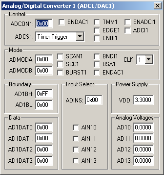
Analog Digital Converter 1 Dialog

The Analog/Digital Converter (ADC) dialog displays and configures the A/D converter. The controls in this dialog are separated into several logical groups.
Control Group
- ADCON1 contains the following ADC control register settings:
- ENADC1 (Enable ADC Channel) is set to enable ADC1.
- TMM1 (Timer Trigger Mode 1) is set to start conversion when Timer 1 overflows.
- EDGE1 (Rising Edge Start) is set to start conversion on a rising edge of external interrupt 1 input (P1.4). If reset, conversion starts on the falling edge of P1.4.
- ENBI1 (Enable A/D Boundary Interrupt 1) is set to trigger an interrupt if the boundary interrupt flag is set when an A/D conversion completes.
- ENADCI1 (ADC Conversion Complete Interrupt Enable) is set to enable the A/D conversion complete interrupt.
- ADCI1 (ADC Interrupt) is set when an A/D conversion completes. This bit must be cleared by software.
- ADCS1 (A/D Conversion Started Mode) selects Timer Trigger, Immediate, Edge trigger or Dual Immediate Start mode.
Mode Group
- ADM1DA (A/D Mode Register A) contains the following ADC mode register settings for ADC 1:
- SCAN1 is set for single conversion mode.
- SCC1 is set for fixed channel, continuous conversion mode.
- BURST1 is set for auto scan, continuous conversion mode.
- BNDI1 (ADC Boundary Flag) is set to indicate that conversion result is outside of the limits defined by the boundary registers.
- ADM1DB (A/D Mode Register B) contains the following ADC mode register settings for ADC 1:
- BSA1 (Boundary Select All) is set to set the boundary flag (BNDI1) if any of the 4 ADC1 inputs exceed the boundary limits. When reset, the boundary flag (BNDI1) is set if only the AD00 input exceeds the boundary limits.
- ENDAC1 (Enable DAC) is set to enable the DAC mode for ADC 1.
- CLK (ADC Clock Divider) is the value divided into the CPU clock (CCLK) to produce the ADC clock.
Boundary Group
- AD1BH (ADC1 Boundary High Register) is the highest converted value allowed.
- AD1BL (ADC1 Boundary Low Register) is the lowest converted value allowed.
Data Group
- AD1DATx displays the converted value for channel x.
Input Select Group
- ADINS (Analog Input Select Register) contains the following analog input selection bits:
- AIN1x (Enable Analog Input x) is set to enable pin AD1x) for conversion.
Power Supply Group
- VDD contains the input reference voltage at the VDD pin.
Analog Voltages Group
- AD1x (Analog Input Channels x) displays the analog voltage value input for pin AD1x.
ADx VTREG
Data Type: float
The ADx VTREGs set the analog input voltages for simulated A/D converters. The ADx VTREGs represent the inputs to the analog input pins of the MCU for analog input 0, 1, 2, and so on. AD0 sets the input voltage for analog input #0, AD1 sets the input voltage for analog input #1, etc. If you have properly configured the analog inputs, the following commands (typed in the debugger's Command Window) input the voltages specified.
AD0 = 0.000  /* Analog Input 0 = 0.000 volts */
AD1 = 2.500  /* Analog Input 1 = 2.500 volts */
AD2 = 4.999  /* Analog Input 2 = 4.999 volts */
You may also enter the analog input voltages using the A/D Converter Dialog which is accessable from the Peripherals menu. You may create a debugger signal function to periodically change the value of the A/D input. The following signal function increases the A/D Channel 1 input voltage by 0.1 volts each second.
signal void AD1_sig (void) {
float f;

for (f = 0.0; f < 5.0; f += 0.1)
  {
  swatch (1.0);                  // Delay 1 second
  AD1 = f;                      // Set AD1 Voltage
  }
}
ProductsDevelopment Tools |
Hardware & Collateral |
Downloads |
Support |
Contact |
