|
||
| Products Download Events Support Videos | ||
Product Information
Device Database®
Downloads
Compliance Testing
Distributors
Peripheral Simulation
For Analog Devices ADuC7026 — Analog/Digital Converter (12 Channels)
Simulation support for this peripheral or feature is comprised of:
- Dialog boxes which display and allow you to change peripheral configuration.
- VTREGs (Virtual Target Registers) which support I/O with the peripheral.
These simulation capabilities are described below.
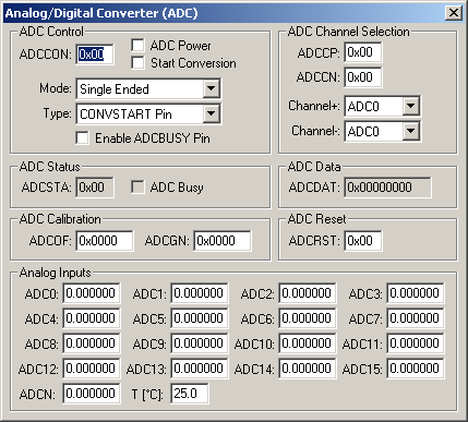
Analog/Digital Converter Dialog

The Analog/Digital Converter (ADC) dialog displays and configures the A/D converter. The controls in this dialog are separated into several logical groups.
ADC Control Group
- ADCCON contains the ADC control register settings.
- Mode selects single-ended, differential or pseudo-differential mode.
- Type selects the conversion input type (CONVSTART, Timer 2, Timer 3, Single Software, Continuous Software or PLA).
- Enable ADCBUSY Pin is set to manually enable ADCBUSY.
ADC Channel Selection Group
- ADCCP (Positive ADC Channel Selection Register) contains the value of the positive channel selection register (Channel+) below.
- ADCCN (Negative ADC Channel Selection Register) contains the value of the negative channel selection register (Channel-) below.
- Channel+ selects a positive ADC channel.
- Channel- selects a negative ADC channel.
ADC Status Group
- ADCSTA (ADC Status Register) indicates when the ADC conversion result is ready.
- ADC Busy is set while the ADC is performing a conversion and reset when the conversion is complete.
ADC Data Group
- ADCDAT (ADC Data Result Register) contains the 12-bit digital conversion result.
ADC Calibration Group
- ADCOF (ADC Offset Calibration Register) contains the 10-bit value used for ground reference calibration.
- ADCGN (ADC Gain Calibration Register) contains the 10-bit value used for reference voltage (VREF) calibration.
ADC Reset Group
- ADCRST (ADC Reset Register) resets all the ADC registers to default values.
Analog Inputs Group
- ADC0-ADC15 (Analog Input Channels 0-15) displays the analog voltage value input for each channel.
- ADCN (ADCNEG) displays the bias point or negative analog input of the ADC in pseudo-differential mode. It must be connected to the ground of the signal to convert.
- T[°C] (Temperature) displays the on-chip (die) temperature.
ADCN VTREG
Data Type: float
ADCNEG Input Voltage Bias point or Negative Analog Input of the ADC in pseudo differential mode. Must be connected to the ground of the signal to convert. This bias point must be between 0V and 1V.
ADCx VTREG
Data Type: float
The ADCx VTREGs set the analog input voltages for simulated A/D converters. The ADCx VTREGs represent the inputs to the analog input pins of the MCU for analog input 0, 1, 2, and so on. ADC0 sets the input voltage for analog input #0, ADC1 sets the input voltage for analog input #1, etc. If you have properly configured the analog inputs, the following commands (typed in the debugger's Command Window) input the voltages specified.
ADC0 = 0.000  /* Analog Input 0 = 0.000 volts */
ADC1 = 2.500  /* Analog Input 1 = 2.500 volts */
ADC2 = 4.999  /* Analog Input 2 = 4.999 volts */
You may create a debugger signal function to periodically change the value of the A/D input. The following signal function increases the A/D Channel 1 input voltage by 0.1 volts each second.
signal void ADC1_sig (void) {
float f;

for (f = 0.0; f < 5.0; f += 0.1)
  {
  swatch (1.0);                  // Delay 1 second
  ADC1 = f;                      // Set ADC1 Voltage
  }
}
ProductsDevelopment Tools |
Hardware & Collateral |
Downloads |
Support |
Contact |
