|
||
| Products Download Events Support Videos | ||
Product Information
Device Database®
Downloads
Compliance Testing
Distributors
Peripheral Simulation
For Analog Devices ADuC7026 — Digital/Analog Converter 1
Simulation support for this peripheral or feature is comprised of:
- Dialog boxes which display and allow you to change peripheral configuration.
- VTREGs (Virtual Target Registers) which support I/O with the peripheral.
These simulation capabilities are described below.
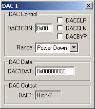
DAC 1 Dialog

The DAC 1 dialog displays and configures the Digital/Analog converter. The controls in this dialog are separated into several logical groups.
DAC Control Group
- DAC1CON (Control Register) displays and configures the D/A Converter control register.
- DACCLR (DAC Clear) is set to enable normal DAC operation. If reset, the data register of the DAC is set to zero.
- DACCLK (DAC Update Rate) is set to update the DAC using Timer 1. If reset, the core clock is used.
- DACBYP (Buffer Bypass) is set to bypass the output buffer. Resetting this bit buffers the DAC output.
- Range (DAC Range Setting) selects the voltage range.
DAC Data Group
- DAC1DAT (Data Register) contains the 12-bit digital data to be converted.
DAC Output Group
- DAC1 (Output Register) displays the converted analog voltage value.
DACREF VTREG
Data Type: float
DACREF Pin Voltage
DACx VTREG
Data Type: float
DAC0 Output Voltage
ProductsDevelopment Tools |
Hardware & Collateral |
Downloads |
Support |
Contact |
