|
||
| Products Download Events Support Videos | ||
Product Information
Device Database®
Downloads
Compliance Testing
Distributors
Peripheral Simulation
For Silicon Laboratories, Inc. C8051F330 — D/A Converter (10-bit)
Simulation support for this peripheral or feature is comprised of:
- Dialog boxes which display and allow you to change peripheral configuration.
- VTREGs (Virtual Target Registers) which support I/O with the peripheral.
These simulation capabilities are described below.
Digital / Analog Converter Dialog

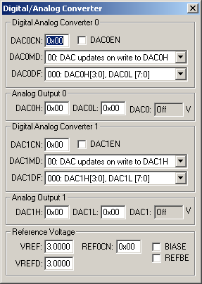
The Digital/Analog Converter dialog displays and configures simulation capabilities of the two Digital/Analog Converters. The controls in this dialog are separated into several logical groups.
Digital/Analog Converter 0
- DAC0CN (DAC 0 Control Register) displays and configures the D/A Converter control register.
- DAC0EN (DAC 0 Enable) enables DAC 0 operation.
- DAC0MD (DAC 0 Mode) determines when the DAC output is updated, based on either a write to DAC0 or when Timer 2, 3 or 4 overflows.
- DAC0DF (DAC Data Format) determines the position of the 12-bit digital output within a 16-bit word.
Analog Output 0
- DAC0H (DAC Data Output - High byte) is the MSB of the DAC output word.
- DAC0L (DAC Data Output - Low byte) is the LSB of the DAC output word.
- DAC0 (Output Register) displays the converted analog voltage value.
Digital/Analog Converter 1
- DAC1CN (DAC 1 Control Register) displays and configures the D/A Converter control register.
- DAC1EN (DAC 1 Enable) enables DAC 1 operation.
- DAC1MD (DAC 1 Mode) determines when the DAC output is updated, based on either a write to DAC1 or when Timer 2, 3 or 4 overflows.
- DAC1DF (DAC Data Format) determines the position of the 12-bit digital output within a 16-bit word.
Analog Output 1
- DAC1H (DAC Data Output - High byte) is the MSB of the DAC output word.
- DAC1L (DAC Data Output - Low byte) is the LSB of the DAC output word.
- DAC1 (Output Register) displays the converted analog voltage value.
Reference Voltage
- VREF contains the bandgap output reference voltage.
- VREFD contains the voltage at the DAC voltage reference input pin.
- REF0CN (Reference Control Register) contains the following controls:
- BIASE (Bias Generator Enable) is set to enable internal bias voltage generation.
- REFBE (Reference Buffer Enable) is set to use the VREF pin to drive the internal voltage reference.
DAC0 VTREG
Data Type: float
The DAC0OUT VTREG represents the analog output voltage for simulated D/A converter. The DAC0OUT VTREG represents the outputs from the DAC 0 output pin of the MCU.
ProductsDevelopment Tools |
Hardware & Collateral |
Downloads |
Support |
Contact |
