|
||
| Products Download Events Support Videos | ||
Product Information
Device Database®
Downloads
Compliance Testing
Distributors
Peripheral Simulation
For Infineon C515A-L — A/D Converter (10-bit, 8 channels)
Simulation support for this peripheral or feature is comprised of:
- Dialog boxes which display and allow you to change peripheral configuration.
- VTREGs (Virtual Target Registers) which support I/O with the peripheral.
These simulation capabilities are described below.
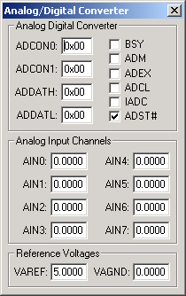
Analog/Digital Converter Dialog

The Analog/Digital Converter dialog displays and configures the A/D converter. The controls in this dialog are separated into several logical groups.
Analog/Digital Converter Group
- ADCON0 (ADC Control Register 0) contains the Interrupt (IADC), Busy (BSY) and Mode (ADM) status.
- ADCON1 (ADC Control Register 1) contains the conversion clock prescaler settings (ADCL0) and ADCL1).
- ADDATH (A/D Converted Data - High byte) contains the most significant 8-bits of the 10-bit A/D conversion result.
- ADDATL (A/D Converted Data - Low byte) contains the least significant 2-bits of the 10-bit A/D conversion result.
- BSY (Busy Flag) is hardware controlled and is set when an A/D conversion is in progress.
- ADM (A/D Mode) is set to trigger a new A/D conversion automatically (Continuous Mode). If reset, only 1 value is converted (Single Conversion Mode). Resetting this bit stops A/D conversion when the current conversion completes.
- ADEX (External Start) when set, uses the falling edge of P4.0 (ADST) to start an A/D conversion.
- ADCL (A/D Conversion Clock Ratio 1) used with ADCL0 to determine the prescaler ratio for the A/D conversion clock. This bit is reset by default.
- IADC (A/D Converter Interrupt Request Flag) is set by the hardware when an A/D conversion completes. It must be reset by software.
- ADST# (External Start Pin) reflects the value of P4.0 (ADST) signal level.
Analog Input Channels Group
- AIN0-AIN3 (Analog Input Channels 0-3) are used for setting voltage input to the ADC. These 4 inputs are alternate functions for Port pins P1.0-P1.3. The text box displays the analog voltage value for each input channel.
- AIN4-AIN7 (Analog Input Channels 4-7) are used for setting voltage input to the ADC. These 4 inputs are alternate functions for Port pins P3.2-P3.5. The text box displays the analog voltage value for each input channel.
Reference Voltages Group
- VAREF (A/D Reference Voltage) contains the maximum voltage value allowed for A/D conversion. When the analog input value exceeds this value, the digital result is 0x3FF.
- VAGND (A/D Reference Ground) contains the minimum voltage value allowed for A/D conversion. When input voltage is below this value, the digital result is 0x0000.
AINx VTREG
Data Type: float
The AINx VTREGs set the analog input voltages for simulated A/D converters. The AINx VTREGs represent the inputs to the analog input pins of the MCU for analog input 0, 1, 2, and so on. AIN0 sets the input voltage for analog input #0, AIN1 sets the input voltage for analog input #1, etc. If you have properly configured the analog inputs, the following commands (typed in the debugger's Command Window) input the voltages specified.
AIN0 = 0.000  /* Analog Input 0 = 0.000 volts */
AIN1 = 2.500  /* Analog Input 1 = 2.500 volts */
AIN2 = 4.999  /* Analog Input 2 = 4.999 volts */
You may also enter the analog input voltages using the A/D Converter Dialog which is accessable from the Peripherals menu. You may create a debugger signal function to periodically change the value of the A/D input. The following signal function increases the A/D Channel 1 input voltage by 0.1 volts each second.
signal void AIN1_sig (void) {
float f;

for (f = 0.0; f < 5.0; f += 0.1)
  {
  swatch (1.0);                  // Delay 1 second
  AIN1 = f;                      // Set AIN1 Voltage
  }
}
VAGND VTREG
Data Type: float
The VAGND VTREG contains the A/D Reference Ground (the minimum voltage allowed for A/D conversions). When an A/D input voltage is below this value, the digital result is 0x0000.
VAREF VTREG
Data Type: float
The VAREF VTREG contains the A/D Reference Voltage (the maximum voltage allowed for A/D conversions). When the analog input value exceeds this value, the digital result is 0x3FF.
ProductsDevelopment Tools |
Hardware & Collateral |
Downloads |
Support |
Contact |
