|
||
| Products Download Events Support Videos | ||
Product Information
Device Database®
Downloads
Compliance Testing
Distributors
Peripheral Simulation
For Silicon Laboratories, Inc. C8051F120 — Temperature Sensor
Simulation support for this peripheral or feature is comprised of:
- Dialog boxes which display and allow you to change peripheral configuration.
- VTREGs (Virtual Target Registers) which support I/O with the peripheral.
These simulation capabilities are described below.
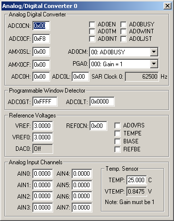
Analog/Digital Converter 0 Dialog

The Analog/Digital Converter (ADC) dialog displays and configures the A/D converter. The controls in this dialog are separated into several logical groups.
Analog Digital Converter
- ADC0CN contains the following ADC control register settings:
- ADC0EN (ADC0 Enable) is set to enable the A/D converter.
- ADC0TM (ADC Track Mode) is set to enable low-power track and hold mode.
- ADC0INT (ADC Interrupt) is set when an A/D conversion completes.
- ADC0BUSY (ADC Busy) is set when and A/D conversion is in progress.
- ADC0WINT (ADC Window Compare Interrupt) is set when a Window Comparison Match occurs.
- ADC0LJST (Left Justify Select) is set to left-justify the ADC0H and ADC0L register. If reset, they are right-justified.
- ADC0CF contains the SAR Clock and PGA ADC control register settings.
- ADC0CM (ADC Conversion Mode) selects the event that starts the A/D conversion.
- AMX0SL (Channel Select Register) is used to select the ADC input.
- AMX0CF (AMUX0 Configuration Register) configures the analog inputs for differential (bit = 1) or single-ended (bit = 0). Only bits 0-3 are used.
- PGA0 (ADC Internal Amplifier Gain) selects the gain value for the internal amplifier (PGA).
- ADC0H (ADC High-Order Data Word) contains the MSB of the 10-bit ADC result. AD0LJST affects where data is located in this byte.
- ADC0L (ADC Low-Order Data Word) contains the LSB of the 10-bit ADC result. AD0LJST affects where data is located in this byte.
- SAR Clock 0 displays the calculated SAR (Successive Approximation Register) clock value derived from the system clock and bits 7-3 in ADC0CF.
Programmable Window Detector This feature continuously compares the output of the ADC to the following limit registers and notifies the system when an ADC output falls outside of this range:
- ADC0GT (Greater Than Data High Byte Register) is the high limit reference value.
- ADC0LT (Less Than Data High Byte Register) is the low limit reference value.
Reference Voltages
- VREF contains the bandgap output reference voltage.
- VREF0 contains the voltage at the ADC voltage reference input pin.
- DAC0 (D/A Output Reference) displays the voltage output from the D/A converter.
- REF0CN (Reference Control Register) contains the following controls:
- AD0VRS (ADC Voltage Reference Select) is set to use the DAC0 output voltage in place of the VREF0 voltage for VREF.
- TEMPE (Temperature Sensor Enable) is set to enable the internal temperature sensor.
- BIASE (Bias Generator Enable) is set to enable internal bias voltage generation.
- REFBE (Reference Buffer Enable) is set to use the VREF pin to drive the internal voltage reference.
Analog Input Channels
- AINx (Analog Input Channels x) displays the analog voltage value input for each channel.
Temp. Sensor
- TEMP (Temperature) displays the on-chip (die) temperature.
- VTEMP (Temperature Output Voltage) is the the voltage input to the PGA when the Temperature Sensor is selected.
VTEMP VTREG
Data Type: float
VTEMP is the the voltage input to the PGA when the Temperature Sensor is selected.
ProductsDevelopment Tools |
Hardware & Collateral |
Downloads |
Support |
Contact |
